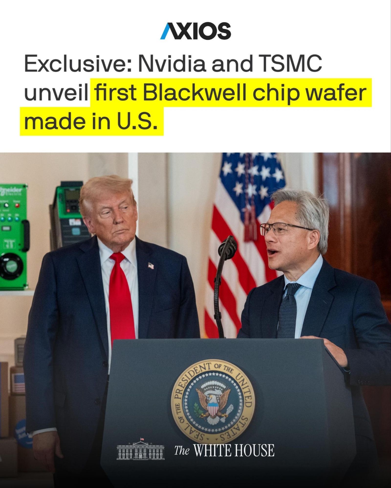
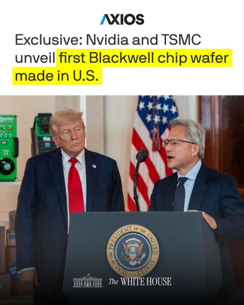
PHOENIX, ARIZONA Oct 19, 2025 – In a landmark moment for American semiconductor manufacturing, Nvidia and Taiwan Semiconductor Manufacturing Company (TSMC) announced the completion of the first U.S.-produced wafer destined to become Blackwell AI chips, marking a significant step toward re-shoring critical technology production. The unveiling, conducted at TSMC’s state-of-the-art facility in Phoenix, Arizona, was attended by Nvidia CEO Jensen Huang and underscored the Trump administration’s push for domestic AI infrastructure.
The event, exclusively revealed to Axios, featured Huang addressing workers and dignitaries, praising the facility’s output as “the single most important chip… now being produced in America.” Standing before a gleaming wafer under the American flag, Huang credited President Donald J. Trump’s policies for enabling this breakthrough, calling it “just the beginning” of a broader AI manufacturing renaissance in the U.S.
“This is historic,” Huang declared, his voice echoing through the cleanroom. “You built something incredible, but you will realize in time that you are part of something historic.” He emphasized the wafer’s role in powering the next generation of artificial intelligence, from data centers to advanced computing, and positioned it as foundational for U.S. leadership in the global AI race.
In a joint statement, Nvidia and TSMC highlighted their collaboration: “Nvidia and TSMC are working together to build the infrastructure that powers the world’s AI factories, right here in America.” The companies projected that the Arizona plant alone would generate thousands of high-tech jobs and draw a constellation of suppliers, bolstering the domestic ecosystem.
The announcement aligns with the administration’s aggressive incentives under the CHIPS and Science Act, expanded during Trump’s second term to accelerate onshoring. Trump, who joined Huang for a ceremonial photo op at the White House earlier in the week, has touted such developments as key to economic sovereignty and national security. “Today we’ve laid the foundation [for the U.S.] to lead the AI race at the infrastructure level,” Huang added, directly nodding to the president’s vision.
Looking ahead, Nvidia plans to invest a staggering half-trillion dollars in AI-related infrastructure over the coming years, with TSMC’s Arizona expansion—now in Phase 2—expected to ramp up production of advanced nodes by 2027. While full-scale chip fabrication remains years away, industry analysts view this wafer as a proof-of-concept that could reduce U.S. reliance on overseas supply chains, particularly amid geopolitical tensions with China.
The White House amplified the news on X, posting a photo of Trump and Huang with the caption “MADE IN AMERICA 🇺🇸,” which quickly garnered thousands of likes and shares. Supporters hailed it as a “Trump win for tech dominance,” while critics noted the project’s roots in Biden-era legislation.
As the U.S. vies for supremacy in semiconductors—projected to underpin a $1 trillion AI market by 2030—this Phoenix milestone signals a pivot from offshoring to innovation at home, potentially reshaping global tech dynamics.
This report draws from Axios reporting and the official White House X post.